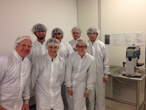
Caption: Back row: Michael Drews, Javier Cardenas, Carl Bunker-Peterson, Girard Clemons. Front row: Zasadzinski, Jonathan Volker, Carly Ilg
A group of six IIT freshman physics majors received a tour of Microlink, a semiconductor manufacturer in Niles, IL, that makes high-efficiency solar cells as well as high-speed transistors for cellular phones. The tour was part of their PHYS 100 course (Introduction to the Professions), taught by physics Professor John Zasadzinski.
The solar cells achieve the high efficiency by stacking layers of different GaAs alloys which have unique energy band gaps and are thus sensitive to different frequency bands of the solar spectrum, thereby capturing more of the light.
The students learned about the growth if GaAs films using the technique of chemical vapor deposition (CVD), a method invented by an IIT chemistry alum, Harold Manasevit (Ph.D. ’59). The processing of devices is done in a clean room environment requiring the donning of “bunny suits” prior to entering the fabrication facility.
